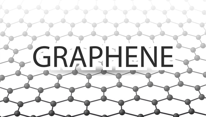
Two-dimensional material research is of great value and has a wide range of downstream applications
Nanomaterials can be divided into zero-dimensional materials, one-dimensional materials, two-dimensional materials, and three-dimensional materials. Two-dimensional materials, the full name of two-dimensional atomic crystal materials, are materials in which electrons can move freely (planar motion) only on the nanometer scale (1-100nm) in two dimensions. The concept of two-dimensional materials was proposed in 2004 with the birth of graphene. In addition to graphene, representative products of two-dimensional materials include transition metal sulfides (such as molybdenum disulfide, tungsten disulfide, tungsten diselenide, Molybdenum selenide), boron nitride, MXene, black phosphorus, etc.
The thickness of two-dimensional materials is ultra-thin, and their carrier migration and heat diffusion are all within the two-dimensional plane, which has the advantage of ultra-high carrier mobility. The band gap, electron spin, and valley degrees of freedom of two-dimensional materials can be controlled and usually have excellent electrical or optical properties. Based on the above characteristics, two-dimensional materials are one of the research hotspots in the fields of physics, chemistry, materials science, etc., especially two-dimensional materials with semiconductor properties, which can be used as high-mobility channel materials to reduce transistor size and improve integration. It has important research value in terms of circuit performance.
According to the “Research Report on Application Market Demand and Development Opportunities of China’s Two-dimensional Material Industry from 2022 to 2027” released by the Industrial Research Center, Two-dimensional materials can be used to manufacture field effect transistors, diodes, photodetectors, PN homojunction semiconductors, PN heterojunction semiconductors, transparent conductive electrodes, memristors, LEDs, solar cells, electro-photocatalysts, etc. The main research areas of two-dimensional materials with semiconductor properties are concentrated in the fields of high-performance field effect transistors, high-performance PN junction photodetectors, and two-dimensional material heterojunctions. Theoretically, two-dimensional materials can be used in a wide range of fields such as integrated circuits, semiconductors, electronics and electronics, display lighting, and new energy.
In quantum computing, qubits are units of quantum information. Reducing the size of qubits while ensuring performance can further improve the performance of quantum computers and develop smaller quantum devices. In January 2022, researchers at the Massachusetts Institute of Technology in the United States used the two-dimensional material hexagonal boron nitride as a superconducting qubit to build a smaller capacitor, reducing the qubit’s footprint by twofold without sacrificing performance. orders of magnitude. This provides new technical support for the development of the quantum computing industry.
Industry analysts said that as research continues to deepen, the number of preparation methods for two-dimensional materials continues to increase, mainly including mechanical peeling methods, liquid Phase exfoliation method, vapor deposition method, wet chemical synthesis method, organic conversion method, etc. Different two-dimensional material preparation methods have their own advantages and disadvantages. Due to problems such as difficulty in large-scale preparation, low preparation efficiency, easy generation of defects, easy introduction of impurities, difficulty in controlling product composition, and high environmental requirements, at present, most two-dimensional materials The preparation method is still only used in the laboratory field and cannot be transformed into industrialization. New preparation processes are still under continuous research and exploration.

 微信扫一扫打赏

